JFET-MOSFET Power Amplifier
Welcome to mosfet lover community
JFET-MOSFET Power Amplifier
Ir. F. Didik Wiryawan Adhi Prasetya
Jakarta, Indonesia
A lovely country with endless attraction.
In the era of ’70 until the end of ’80, the audio amplifier manufacturers competed with each other offerring superior technical specifications in terms of the wide frequency response, total harmonic distortion and intermodulation distortion that under 0.01% (ranging 0.01 to 0001%) and many other things that could be regarded as a ‘selling point’ for each of each brand.
Until now, the technical specifications of the ‘ideal condition’ is still used as a reference.
But among the ‘audiophiles’, especially for the DIYer (Do It Your Self), seemingly the technical specifications of the ‘ideal condition’ will not be used as a single standard, although not to be ignored altogether.
Among this community (audiophiles), the resulting sound to reproduce the original sound is as beautiful as preferred.
It is often found an audio system has a beautiful voice with all the requirements of audiophile, however surprisingly, its common technical specifications are worse than a system of regular ‘HiFi Compo’.
There are 2 different adherents on topology but not necessarily debated:
Adherent 1 : Who need very few components, this may be called ‘minimalist’ or “KISS” (stand for Keep It So Simple) with the goal of natural sounded much less of sound colouration, regardless that the technical specifications are beyond the ideal.
Adherent 2 : Those are idealist design topology very obedient in the text book and an ideal outcome measurement, which resulted in the last chain becomes very complicated and requires many electronic components.
And I may add one more role models are : No minimalist but not too ‘text book minded’, but having a main purpose : to design amplifier having nice and beautiful sound but with the technical requirements which was not too bad.
AMPLFIER with JFET input and MOSFET output. Based on the schematic of a famous Swiss made power amplifier (Goldmund Mimesis3), I did some little modifications on each stage according to my personal taste.
After a long listening, testing and did some changes (tweaking) as well as an understanding of the sound character (a little research and trial), then as the end result, I put it in the design which now named : Mosfet Power Amplifier MP50Di. The Power Amplifier “MP50Di” using JFET (2SK170) in the front end and HITACHI/Renesas Lateral Mosfet (2SK1058/2SJ162) on the amplifier tail end.
Technically, the comparison of performance design using Bipolar Junction Transistor (BJT) and FET / MOSFET will not be much different, but the real difference will be felt at the time of listening especially the clarity and purity sounded on mid and highs region (vocal and acoustic instrument) which is difficult to meet on BJT. There are nuances unique sound that can not be generated by the BJT amplifier.
Design Topology DRAFT.
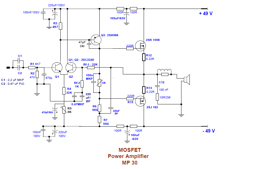
Before entering into a complete range of the MP50Di, it helps us look at the basic topology of this series starts from the most simple.
In addition, it should be noted that this project (especially MP50Di), is not recommended for beginners. Small mistakes made by one who has not had enough experience and do not understand basic circuit work, will result in useless waste of funds. The most basic circuit topology for this design can be seen in Figure-1.
It is a simple 3 stages amplifier:
– input, differential amplifier (or LTP = long-tailed pair),
– VAS (voltage amplifier stage) and
– the amplifier end (with mosfet 2SK1058/2SJ162).
Figure-1 :
The simplicity of the basic design is easily seen on a MOSFET amplifier circuit without including the driver stage.
It is almost impossible for BJT end with this simple design can produce output power of 50W even though half of it.
The output of the differential pair Q1 on Q1 and Q2 (2SC2240), is fed into Q3 (2SA968) which is a VAS with ‘bootstrap’ of R6 and R7.
Q3 is directly driving the final amplifier MOSFETs (K1058 & J162), which can produce up to 100W RMS power output (theoritically), which can not be applied at the BJT end amplifier (because the BJT is ‘current operated devices’ while the Power MOSFET is ‘voltage operated devices’ which does not require large currents to drive it).
Note: Q3 here using 2SA968, a medium power transistor, even though with a small transistor such as 2SA970 (or MPSA92), it can work well without any difference in sound quality. The use of 2SA968 is juts for job security of the device not too close to allowable heat dissipation and easy installation of the heatsink if needed.
Quality Improvement of Phase-1
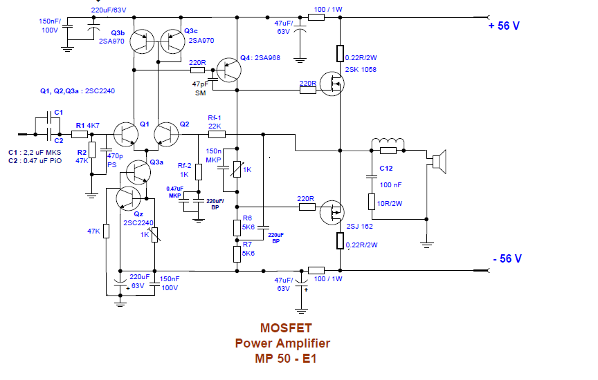
Improved quality of phase-1 was done by adding a constant current source formed by the Q3A and QZ (2SC2240) replaced R4 and R5 and ‘current mirrors’ which is formed by Q3B and Q3C (2SA970) replaced R3.
Figure-2 :
These changes resulted in significant sound quality improvement.
The simplest thing that appeared in the measurement with the DMM (digital multi meter) was the DC offset of 35mV dropped dramatically to about + / – 3.5mV.
The schematic of this improved quality of phase-1 discribed in Figure-2
This circuit is very similar with Project 101 of Rod Elliot of ESP, Australia, the famous simple mosfet amplifier. (http://sound.westhost.com/project101.htm)
Theoretically, this quality improvement (Figure-2) were very influential in improving linearity (also increased in ‘open loop gain’), it was proven in comparative listening test.
Ears fatigue which arise at the time ‘listening’ on previous model, had been greatly reduced here. Music reproduction, sounded more detailed than ever before. Sound staging and clarity were improved compared to previously that had a little noisy because the sound of several musical instruments more likely fight over each other which caused image of ‘position of the music players’ were not definitively clear.
Quality Improvement Phase-2
Although Figure-2 has been producing a quite sufficient sound and can be said to be ‘superior’ than class ‘HiFi Compo’ (even a well-known branded), however driving final amplifier MOSFETs directly from a simple VAS (Voltage Amplifier Stage), has many weaknesses that result in disruption linearity at power levels above 10W (disclaimer : this is on my personal opinion, I didn’t measure it) especially in long enough operation.
This is because the VAS current is very small, less able to do a ‘charge’ and ‘discharge’ to the MOSFETs quickly.
Mosfet amplifier topology without a driver can work very well for the application of class A with low output (let say 10watt) but will be felt weakness on the operation of large power and not a class A (class B).
This weakness is one reason of ‘ears fatigue’ as mentioned above, nevertheless this weakness is only detectable by an experienced audiophile, it is not clearly detectable on measurement equipment (oscilosocope).
Improved quality of phase 2 was done by adding one stage of the driver (Q10 and Q11), 2nd VAS Q6-Q7 with current mirror which is formed by Q8-Q9 and changed the mode of final mosfet from a source follower to become a common source as set out in Figure-3.
Figure 3 :
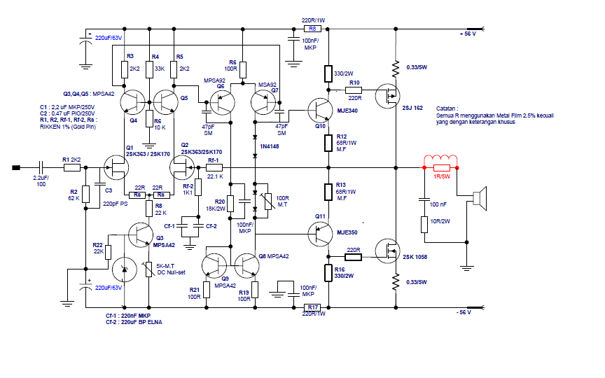 The driver mode is a common emiter and the final is a common-source which both have voltage gain.
With this configuration, the amplifier would give more powerfull and tighter bass (I am a bass lover !)
(Updated July 13th, 2012)
To be honest, this configuration (tail end topology) was inspired by design of David NJ White, “High Quality 100W MOSFET Power Amplifier” (unfortunately, the link : www. wnaudio.com is no longer exist).
The change of simple VAS into differential VAS should also be supported by changed in configuration mode of differential input circuit (input LTP), by changing it from unbalance mode output (single ended) to balance mode output.
Changed in single VAS transistors into a differential VAS (VAS LTP) that loaded by current mirror Q5a and Q4a, providing a significant linearity improvement compared to the composition of the bootstrap R6 and R7 in Figure-1 and Figure-2.
With the high charging speed and discharge, it can achieve good linearity especially when dealing with fast music with dominant high notes.
In addition to change of VAS, the topology at the tail end also be changed which is no longer power follower (no voltage gain) but became a voltage gain circuit.
(July 13th, 2012)
At first glance, you would think of it as a schematic of GoldMund Mimesis3, but please look at the final stage, they are much different of mode. This is a drain follower driven by collector follower (common emitter, Q10-Q11).
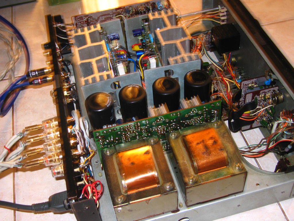
I deliberately chosen the power supply voltage 56V to match my vintage SANSUI AU719 and designed the pcb with dimension matched to the main power unit of AU719. I took off the whole main power amplifier unit AU719 and replaced it with this design that is named MP50Di (stand for Mosfet Power Amplifier 50 watt Didik :p). The amplifier run in class AB with quiescent current 200mA, it is a heavily class AB and quite warm, need fan to cool it down.
Was I happy with this? Yes, of course but not really satisfied yet since I saw there was more able to be done for further improvement.
Further improvement will be coming soon ! 😆
——————————————————————————————————————-
Jakarta, July 6, 2016
Hi Mosfet Lovers !
After 5 years past and my promise, this is the latest version of my MP50Di that can run pure Class A. Difference to the first version is a separated supply rail to enable you to run in pure Class A by reducing voltage rail of the final power mosfet and increasing QCurrent to , depend on the Mosfets are used, 500-1100mA. Using 2SK1058/2SJ162 or BUZ900/905, QC 500mA – 600mA with 32V supply is enough, however if use IRFP240/9240, you need to run hot with 1000-1100mA per device.
VR for unmatched 2SK170 on differential input was added and you can also set its bias to meet your personal taste.
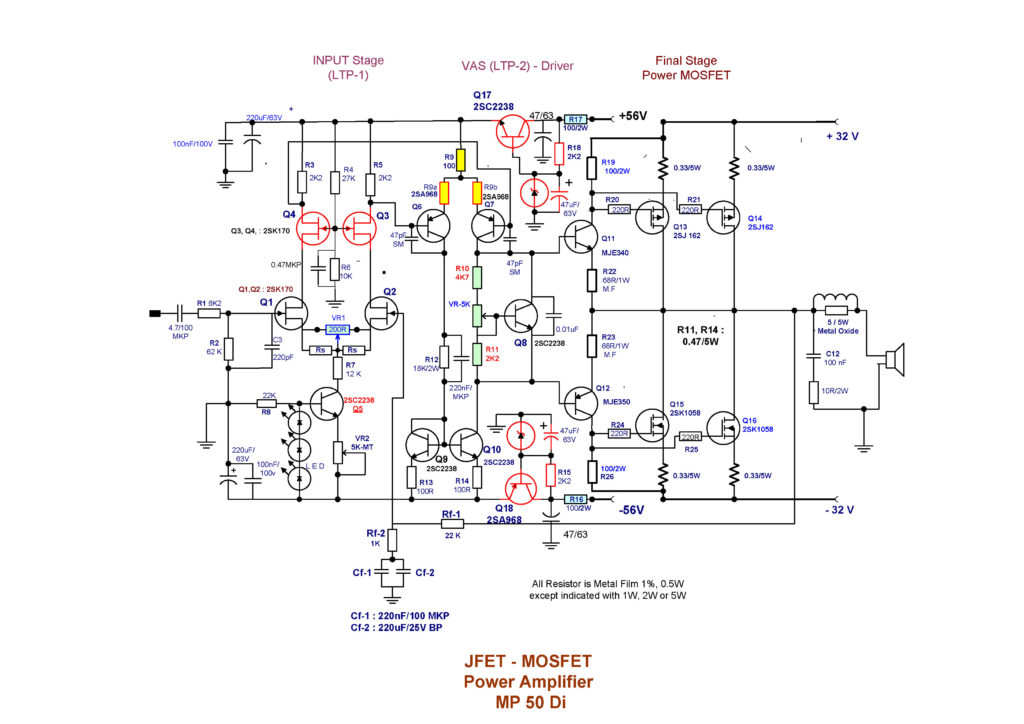
MP50Di ClassA Final Schematic (2014)
Set up manual, will be followed soon…..
 mosfetaudio-didik.com
I already had built a Golmund amp is interested in your pcb thenk you
Hi Huszars,
Sorry for a very late response.
Yes I have the PCB of MP50Di V2, double layer, gold plated.
hI It looks really fine but unfortunately differential pairs are not so
perfect one in case of sounding (analyze limiting RF amplifiers you will find why)
thanks prof uda share. BTW rangkaian ini memang agak ribet ya prof rangkaiannya? Kok saya coba buat rada susah ya? agal terus -_-
Hello
I am very interested in your MP50DI V2 I have the 2SK1058/2SJ162 mosfets original stored from the 1990’s would love to run in Class A.
Do you have PCB’s available, BOM and a parts indicated schematic ?
Please get back to me.
John C.